2D Inductively Coupled Plasma Chamber With Shapes (icpCylShapes.sdf)
Keywords:
- inductively coupled plasma, ICP, discharge, steady state
Problem Description
This VSimPD example illustrates how to simulate an inductively coupled plasma (ICP) in 2D cylindrical coordinates using the VSim Software. ICPs are one of the most common sources used to generate low temperature plasmas, and are extensively used in the semiconductor manufacturing industry. A typical ICP chamber has an antenna external to the plasma powered by an RF current. The plasma is sustained primarily through elecromagnetic induction.
Simulating an inductively coupled plasma is a complex problem. The plasma is electromagnetically driven and inherently three-dimensional. Ordinarily, kinetic modeling of these plasmas would require taking time steps to resolve the speed of light on the computational mesh. These issues are addressed in this example by using a proprietary 2D implicit electromagnetics solver to efficiently model the inductive power source.
This example is an extension of the 2D Inductively Coupled Plasma Chamber, icpCyl.sdf, with the addition of complex material boundary conditions (Shapes) to better define the simulation.
This simulation can be run with a VSimPD license.
Opening the Simulation
The 2D Inductively Coupled Plasma Chamber with Shapes (icpCylShapes.sdf) example is accessed from within VSimComposer by the following actions:
Select the New → From Example… menu item in the File menu.
In the resulting Examples window expand the VSim for Plasma Discharges option.
Expand the Inductively Coupled Plasmas option.
Select 2D Inductively Coupled Plasma Chamber with Shapes and press the Choose button.
In the resulting dialog, create a New Folder if desired, then press the Save button to create a copy of this example.
The resulting Setup Window is shown Fig. 537.
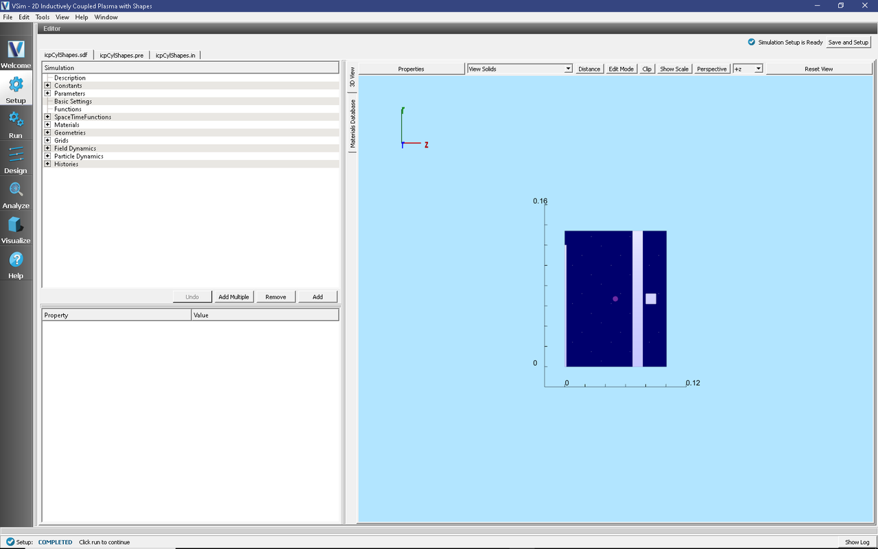
Fig. 537 Setup Window for the icpCylShapes example.
Simulation Properties
This example contains many user defined Constants and Parameters which help simplify the setup and make it easier to modify. The following constants or parameters can be modified by left clicking on Setup on the left-most pane in VSim. Then left click on + sign next to Constants or Parameters and all the constants or parameters used in the simulation will be displayed. To add your own constant or parameter, right click on Constants or Parameters and left click on Add User Defined. Below is an explanation of a few of the constants and parameters used. There are several more constants and parameters included in the simulation, but will not be discussed here for brevity.
I0_RF: Amplitude of RF current source (A)
RF_VOLTAGE: Amplitude of RF voltage source (V)
RF_FREQUENCY: Frequency of the RF sources, same frequency used for current and voltage sources
NDENS: Initial plasma density (#/m^3)
NEUTRALN: Number density of neutral background gas. This determines the mean free path.
BGNZ_ANTENNA, ENDZ_ANTENNA, BGNR_ANTENNA, ENDR_ANTENNA: Location of the antenna in spatial coordinates.
antLength, antWidth, antXPOS, antYPOS: Parameters used to define CSG geometry position of antenna.
There are also many SpaceTimeFunctions (STFunc) defined in this example. BIAS_VOLTAGE and RFsourceSTFuncJ0 are the space-time functions which set the sinusoidal bias voltage and current sources respectively. Note that RFsourceSTFuncJ0 is more complex than BIAS_VOLTAGE to give a smooth ramp for stability.
This example contains 6 specified CSG Geometries, corresponding to a wafer (Silicon dielectric), focusRing (Alumina dielectric), groundShield (Perfect Electric Conductor (PEC)), window (dielectric modeled as bottle glass), antenna (PEC), and biasElectrode (PEC).
These CSG Geometries are defined within VSimComposer by specifying four parameters: Length, Width, XPOS, and YPOS. The type of material needs to also be set. Voltages can be specified on PEC materials as a FieldBoundaryConditions under the Field Dynamics drop down menu. This has been done in icpCylShapes.sdf as dirichletBias - an Electrostatic Dirichlet boundary condition, set to the STFunc BIAS_VOLTAGE for the shape surface object named ‘biasElectrode’.
Running the Simulation
Once finished with the setup, continue as follows:
Proceed to the Run Window by pressing the Run button in the navigation column on the left.
To run the file, click on the Run button in the upper left corner of the
In the Logs and Output Files pane, you will see the text output of the run. The run has completed successfully when you see the output, “Engine completed successfully.” This is shown in Fig. 538.
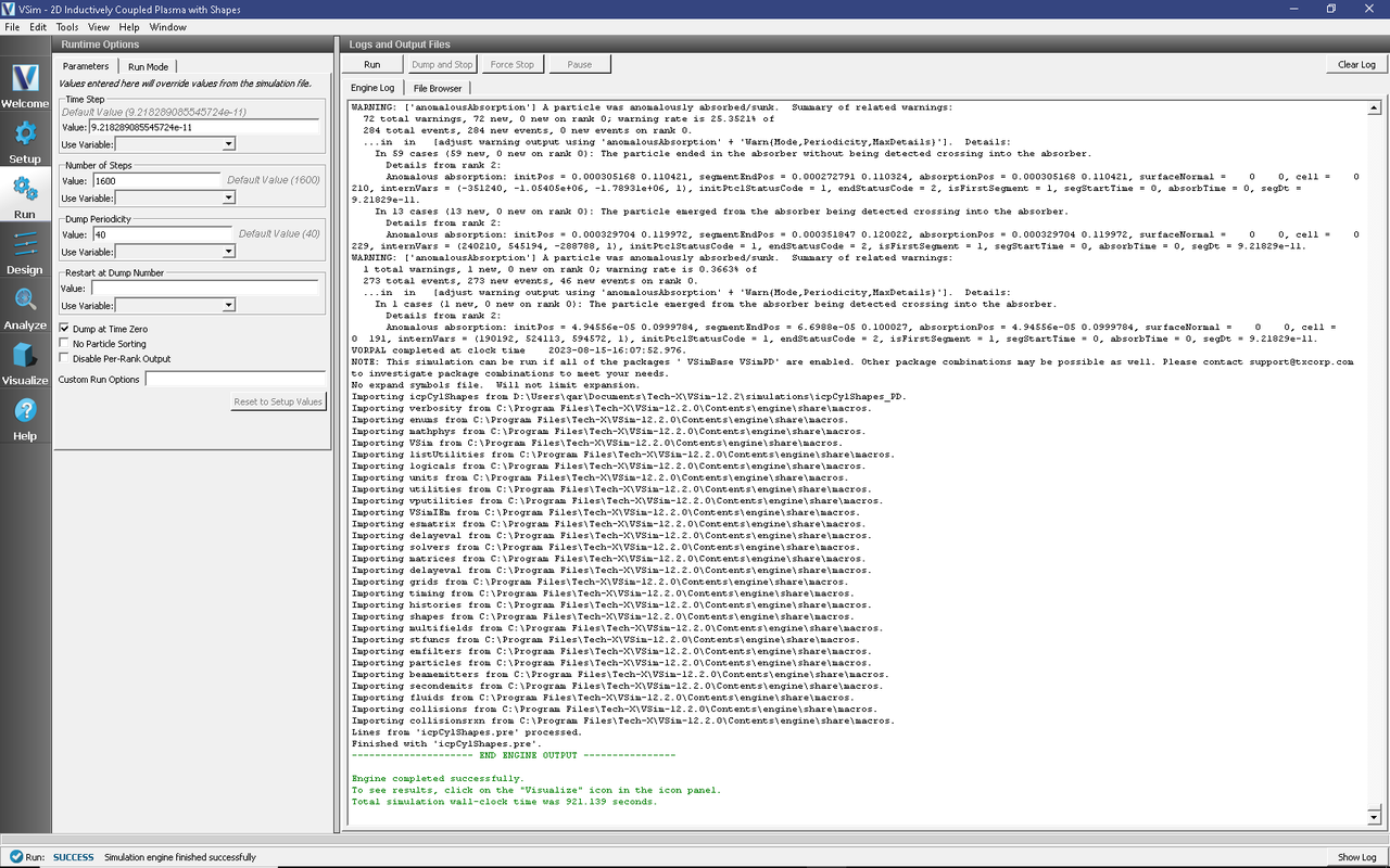
Fig. 538 The Run Window at the end of execution.
Analyzing the Results
After performing the above actions, continue as follows:
Proceed to the Analysis Window by pressing the Analyze button in the navigation column.
In the resulting list of Available Analyzers, select computeAED.py
The analyzer fields should be filled as below:
simulationName :: icpCylShapes [string]
speciesName :: He1 [string]
startTime :: 7.374631e-08 [float]
endTime :: 1.474926e-07 [float]
lowerPos :: 0.001 [float]
upperPos :: 0.1 [float]
historyName :: computeAEDHe1 [string]
numEnergyBins :: 50 [int]
numAngleBins :: 50 [int]
lowerEnergy :: 0 [float]
upperEnergy :: 130 [float]
lowerAngle :: -10 [float]
upperAngle :: 10 [float]
NDIM :: 2 [int]
perpDir :: +z [string]
normTan :: False [bool]
compMajorC :: False [bool]
overwrite :: True [bool]
Click Analyze in the top right corner.
The analsis is completed when you see the output shown in successfully.” This is shown in Fig. 539.
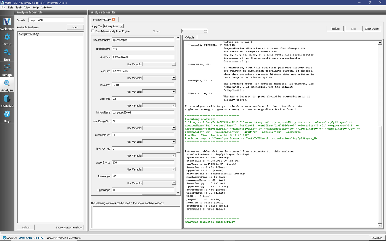
Fig. 539 The Analysis Window at the end of execution.
Visualizing the Results
After performing the above actions, the results can be visualized as follows:
Proceed to the Visualize Window by pressing the Visualize button in the navigation column.
Click on the Add a Data View dropdown menu and select Data Overview.
A Data Overview tab should open, if not already present.
In the Visualization Controls pane, we can select variables for analysis.
View the shapes that are in the simulation by expanding the Geometries menu, and selecting the desired shapes to be drawn (poly (antenna), poly (biasElectrode), poly (focusRing), poly (groundShield), poly (wafer), and poly (window)).
Expand the Scalar Data menu, expand E, and select E_theta to plot the induced azimuthal electric field.
Expand the Particle Data menu, expand the electrons menu, and select electrons_uphi for plotting.
The resulting visualization is shown in Fig. 540 for dump 40.
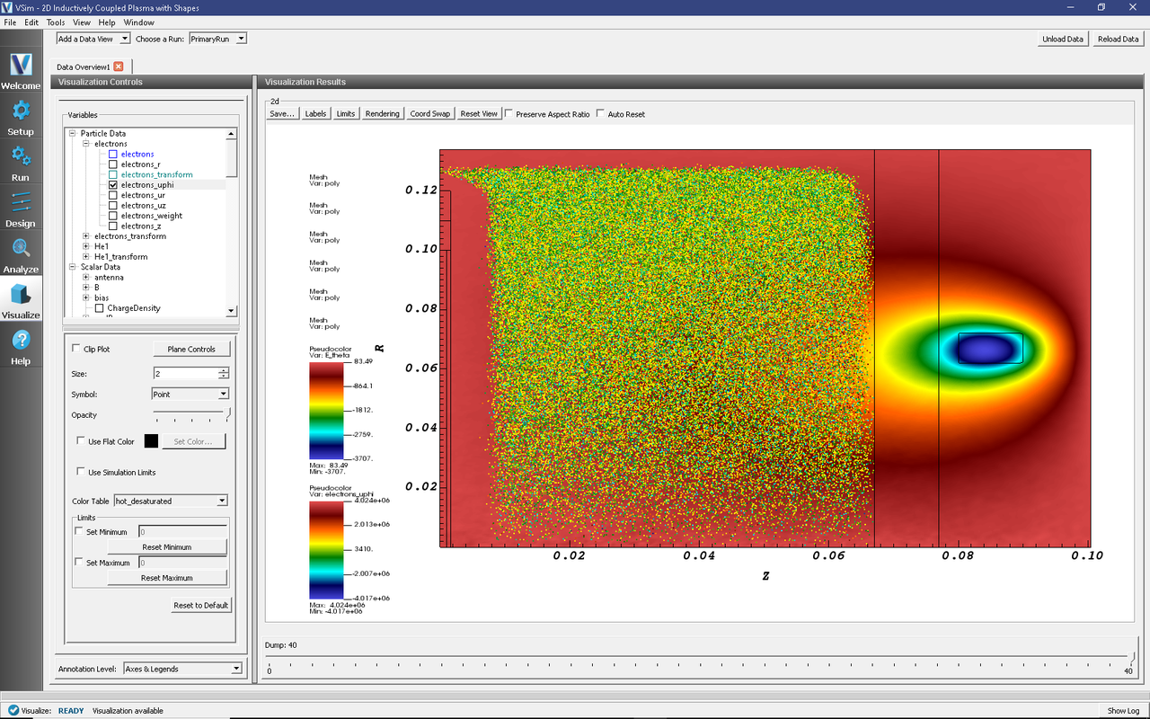
Fig. 540 The azimuthal electric field (E_theta) with electron particle data. Magnitude of the electric field is largest in the current source (antenna) and decays into the plasma as power is absorbed. Electrons are colored by azimuthal velocity.
Additional analysis of the simulation results can be performed as follows:
From the Visualize Window, click on the Add a Data View dropdown menu and select Field Analysis.
A new tab called Field Analysis1 should automatically open.
In the Visualization Controls pane, select the field for analysis, e.g. E_theta.
Perform a lineout by clicking on the Horizontal button and set the intercept to 0.067.
Click the Perform Lineout button and move the Dump silder to progress through time.
The resulting visualization is shown in Fig. 541 for dump 40.

Fig. 541 The azimuthal electric field (E_theta) with a lineout at R = 0.067. Magnitude of the electric field is largest in the current source (antenna) and decays into the plasma as power is absorbed.
To visualize the electric potential:
Go to the Field Analysis1 tab.
In the Visualization Controls pane, select a different field for analysis, this time Phi, the electric potential.
Perform a lineout by clicking on the Horizontal button and set the intercept to 0.067.
Click the Perform Lineout button and move the Dump silder to progress through time.
The resulting visualization is shown in Fig. 542 for dump 35.
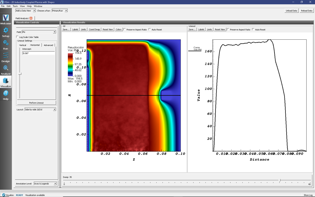
Fig. 542 The electric potential field (Phi) with a lineout at R = 0.067. Sheaths form at the plasma/material boundary surfaces.
Additional data from the simulation was saved as a history file, and can also be viewed:
From the Visualize Window, click on the Add a Data View dropdown menu and select History.
A new tab called History should automatically open.
In the Visualization Results pane, click the Add Window button to add a second window for plotting.
In the top plotting pane, select the Add Curve button.
In the drop down menu, pick the variable for plotting by selecting probePhi.
In the lower plotting pane, select the Add Curve button.
In the drop down menu, pick the variable for plotting by selecting probeE_2.
The resulting visualization is shown in Fig. 543.
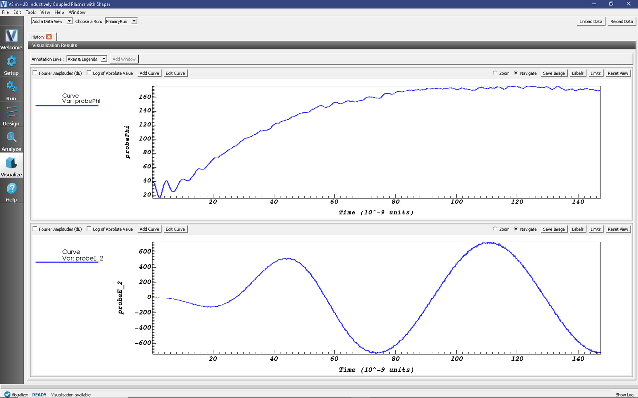
Fig. 543 A time-history of the electric potential (Phi) and the azimuthal electric field at a probe position Z = 0.05 m, R = 0.067 m.
The data generated by the computeAED.py Analyzer can also be visualized:
From the Visualize Window, click on the Add a Data View dropdown menu and select 1-D Fields.
A new tab called 1-D Fields should automatically open.
In the Visualization Results pane, click the Add Window button to add a second window for plotting.
In the top plotting pane, select the Add Curve button.
In the drop down menu, pick the variable for plotting by selecting He1ED.
In the lower plotting pane, select the Add Curve button.
In the drop down menu, pick the variable for plotting by selecting He1AD.
The resulting visualization is shown in Fig. 544.
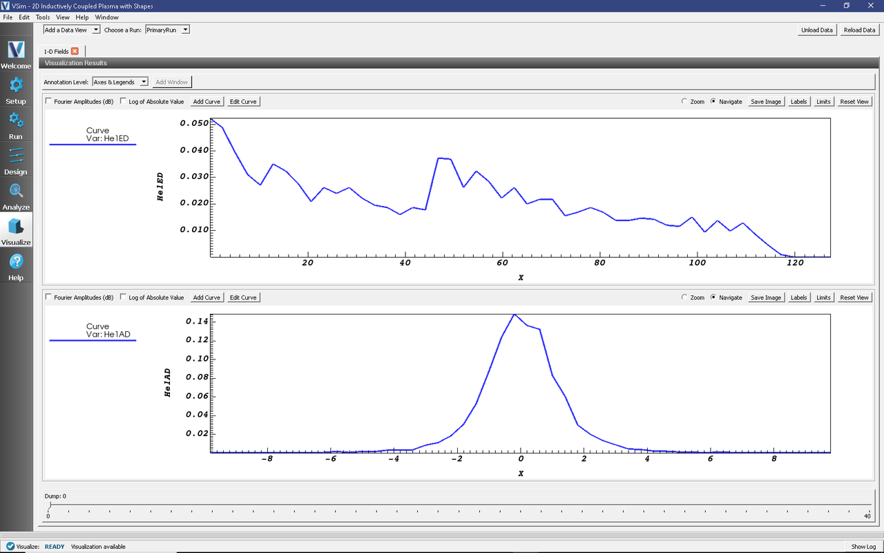
Fig. 544 Images of the Energy Distribution (Top) and the Anguluar Distribution (Bottom) of He1 ions impacting the wafer.
Addition of Bias Voltage
Many inductively coupled plasmas also feature an RF bias, which is simple to add using VSimPD.
Return to the Setup tab.
Under the Simulation window, expand the Parameters menu.
Under Parameters, select RF_VOLTAGE and change the expression from 0. to 100.
Click Save and Setup
Rerun the simulation by going to the Run tab and clicking the Run button.
Plots of the new results can be regenerated following the prior instructions.
The visualization of the Etheta field is shown in Fig. 545 for dump 40.
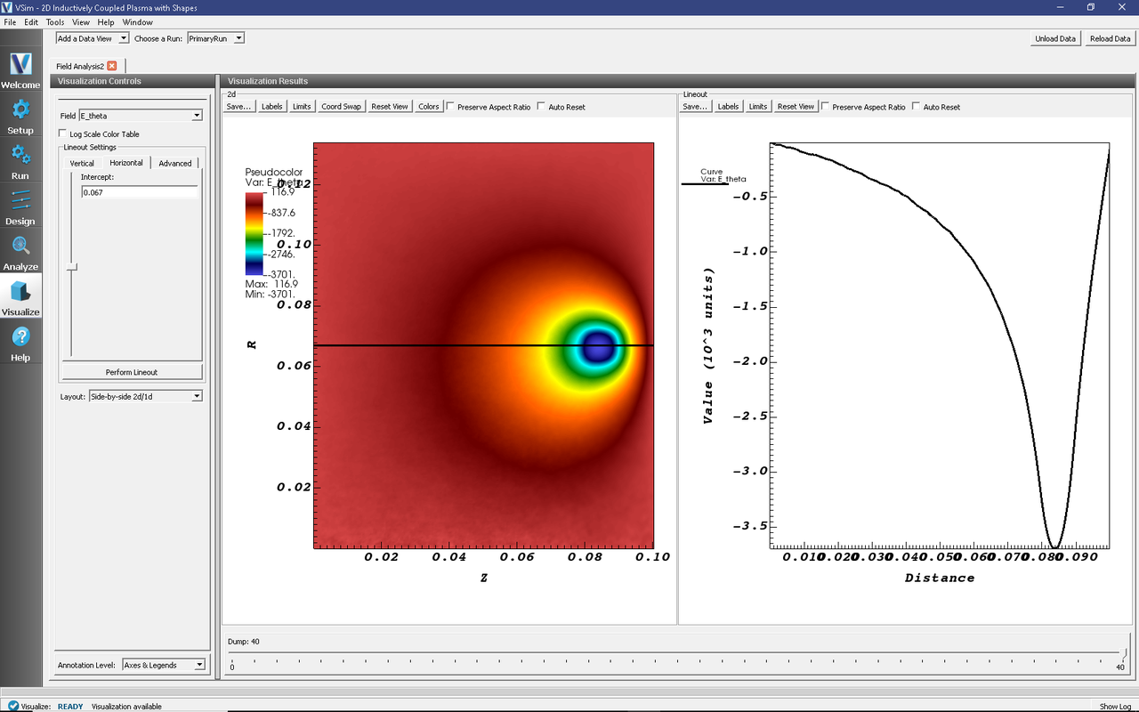
Fig. 545 The azimuthal electric field (E_theta) with a lineout at R = 0.067. Magnitude of the electric field is largest in the current source (antenna) and decays into the plasma as power is absorbed.
The electric potential field is shown in Fig. 546 for dump 35.
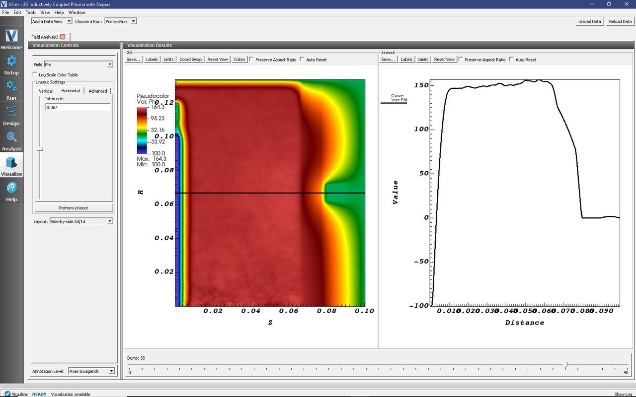
Fig. 546 The electric potential field (Phi) with a lineout at R = 0.067. Sheaths form at the plasma/material boundary surfaces. Dump 35 shows the RF voltage at a minimum, with the lineout showing the potential varying from -100 V on the lower Z boundary, increasing up to 150 V in the plasma, and decreasing inside the dielectrics to 0 V at the uppper Z boundary.
The addition of an RF bias can improve the functionality of an ICP chamber by increasing the energy which ions hit surfaces (Reactive Ion Etching). Voltage for the antenna is set to 0. V, but an applied voltage can additionally be specified if values are known.
The probe at position Z = 0.05 m, R = 0.067 m can also give valuable information about the electrical characteristics of the plasma, and the time series plot is shown in Fig. 547.
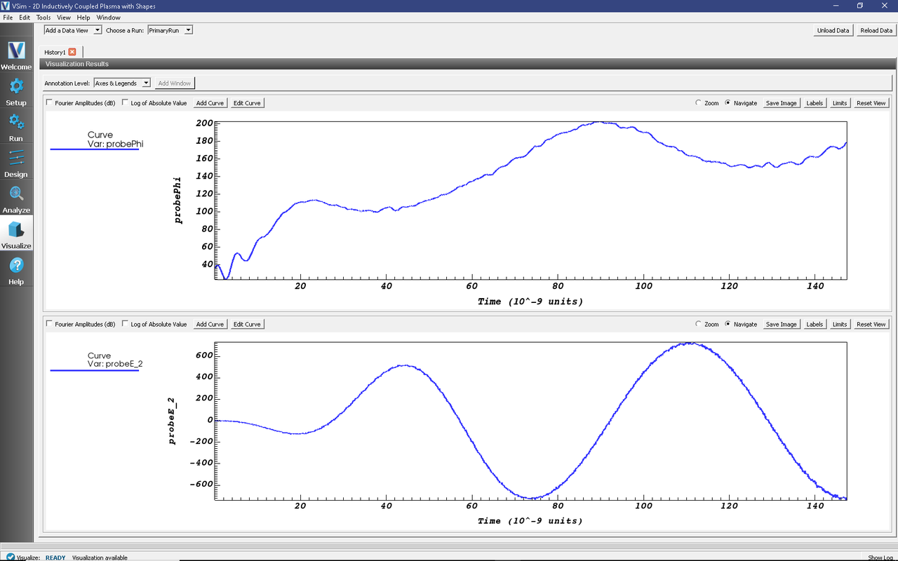
Fig. 547 A time-history of the electric potential (Phi) and the azimuthal electric field at a probe position Z = 0.05 m, R = 0.067 m. The addition of a 100. V RF bias causes the electric potential at the probe position to osciallate and reach a maximum of 200 V compared to 165 V without an applied bias.
Further Experiments
Some of the easier parameters to modify are the RF_VOLTAGE and antenna current, I0_RF. However, it is important to note that the time step and necessary mesh resolution heavily depend on the plasma density for stability. Increasing the antenna current or rf bias voltage can greatly increase the plasma density leading to unstable simulations.
An additional test is to change the placement of the antenna CSG geometry. The position can easily be seen by plotting the poly geometries after a single time-step. The position of the antenna will change where the maximum in the azimuthal E-field occurs, and change how the plasma density profile develops.